Gallium Nitride Semiconductor Device and Substrate Wafer Market Projected for Significant Growth by 2035
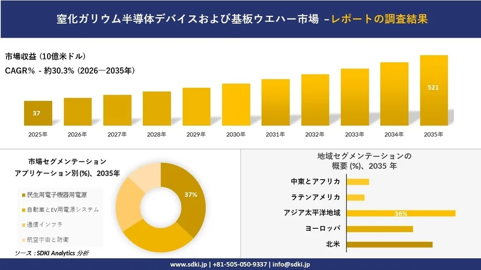
The Gallium Nitride (GaN) semiconductor device and substrate wafer market is poised for substantial expansion, with SDKI Analytics projecting its value to increase from approximately USD 3.7 billion in 2025 to USD 52.1 billion by 2035. This represents a robust Compound Annual Growth Rate (CAGR) of 30.3% over the forecast period.

Driving Forces Behind Market Expansion
The market’s growth is largely attributed to the rapid shift towards high-efficiency power conversion in compact consumer electronic devices. GaN devices offer faster switching speeds and reduced energy loss compared to traditional silicon components, enabling higher frequency operation in chargers and adapters and leading to significant miniaturization of devices. Major electronics manufacturers are increasingly adopting GaN-based fast-charging systems for smartphones, laptops, and wearable devices. This trend creates a strong and sustained demand for both GaN devices and substrate wafers as companies redesign power units to manage heat and enhance charging speeds.
Challenges in GaN Semiconductor Manufacturing
Despite the clear advantages, the GaN semiconductor value chain faces challenges, primarily due to the complexity of manufacturing processes and the high cost of wafer production. Unlike established silicon manufacturing, GaN substrate production requires specialized crystal growth techniques and high-precision processing. These manufacturing complexities can restrict production capacity and slow down large-scale commercialization for certain applications. Device manufacturers must balance performance benefits with increased material and production costs. Scaling up wafer manufacturing economically remains a significant hurdle, affecting pricing and supply stability across the entire GaN ecosystem.
Market Segmentation and Dominant Applications
The market is segmented by application into Consumer Electronics Power Supplies, Automotive and EV Power Systems, Communication Infrastructure, and Aerospace and Defense. The Consumer Electronics Power Supplies segment is expected to hold a dominant revenue share of 37%. This segment continues to be a commercial cornerstone for GaN semiconductor adoption, as thin and compact power adapters and fast chargers directly benefit from GaN’s high switching frequencies and reduced power loss. GaN devices enable manufacturers to miniaturize power designs while improving efficiency, a critical advantage for high-power smartphone and laptop chargers.
Regional Market Dynamics
Asia Pacific is projected to secure the largest revenue share of 36% and demonstrate the fastest growth rate with a CAGR of 32.1%. This is largely due to the region’s dense electronics manufacturing ecosystem, with semiconductor manufacturing, consumer electronics assembly, and communication infrastructure development concentrated in economies such as China, Japan, South Korea, and Taiwan. The expanding electronics manufacturing across the region is accelerating GaN technology adoption in diverse applications, from consumer chargers to communication infrastructure.
Japan’s GaN semiconductor device and substrate wafer market is also expected to expand, offering significant business opportunities. Japan’s leadership in advanced materials science and power electronics engineering is a key driver. The country specializes in upstream and midstream segments of the GaN value chain, focusing on crystal growth, high-purity epitaxial growth, wafer processing techniques, and reliability modeling for next-generation power devices. The increasing adoption of GaN by Japanese automotive, industrial automation, and consumer electronics leaders, aimed at achieving national energy efficiency and electrification goals, makes the domestic ecosystem attractive for material suppliers, equipment manufacturers, and IP-centric technology partners.
Recent Industry Developments
Recent developments in the GaN semiconductor market include:
-
October 2025: imec launched a new industrial program focused on developing 300mm Gallium Nitride (GaN) power electronics technology. This initiative, in collaboration with partners including AIXTRON, GlobalFoundries, KLA, Synopsys, and Veeco, aims to advance GaN epitaxial growth and HEMT process flows on larger diameter wafers, supporting technological innovation in the GaN semiconductor device and substrate wafer market.
-
November 2024: Sumitomo Chemical announced efforts to accelerate mass production technology for 6-inch GaN-on-GaN wafers for power devices. This development highlights increasing investment in high-quality GaN substrates and epitaxial wafer technologies, enabling next-generation power semiconductor devices across automotive, power electronics, and communication sectors.
Key Players in the GaN Market
Prominent global players in the Gallium Nitride semiconductor device and substrate wafer market include:
-
Cree, Inc.
-
Infineon Technologies AG
-
Texas Instruments
-
Qorvo, Inc.
-
STMicroelectronics
Top players in the Japanese market include:
-
Mitsubishi Chemical Corporation
-
Sumitomo Electric Industries, Ltd.
-
Fujitsu Limited
-
Panasonic Holdings Corporation
-
Renesas Electronics Corporation
For more detailed insights, the full market research report is available at:
https://www.sdki.jp/reports/gallium-nitride-semiconductor-devices-and-substrate-wafer-market/59610
A free sample report can be requested here:
https://www.sdki.jp/sample-request-59610
To request a preview of the report:
https://www.sdki.jp/trial-reading-request-59610